
Packaging Automation Overcomes Optoelectronic Component Variety
With the emergence of high-performance digital systems and the rapid growth of Internet traffic in the 1990s, the US Air Force Research Laboratory (AFRL) Micro Electronics Technology Directorate correctly predicted the growing need for optical interconnects and thus initiated several efforts to develop such technologies for the next generation of high-performance digital systems. This work was also prompted by significant advances in optical materials (i.e., III-V materials and polymers), devices (vertical-cavity surface-emitting lasers, VCSELs), and packaging technologies that were also made during this period.1 In collaboration with the Defense Advanced Research Projects Agency (DARPA) Electronic Technology Office, the AFRL thus initiated several major programs in this area.
Purchase SPIE Field Guide to Optical Fiber TechnologyIn this paper, we provide a historical overview of the early pioneering work in the field of VCSEL-based parallel optical links. We also discuss how these efforts have led to the successful commercialization of key optoelectronic components, e.g., VCSEL arrays, ribbon connectors, and detector arrays. Moreover, we present how the development of related low-cost packaging technologies has also been a critical factor in promoting the use of affordable VCSEL-based parallel optical links in intra-data centers.
The first of the AFRL/DARPA programs was a landmark pre-competitive industry effort known as the Optical Electronic Technology Consortium, which consisted of General Electric (GE), AT&T, Honeywell, and IBM. The aim was to develop key optoelectronic components for optical interconnect technology beyond the cost, speed, and density limits of the time. In this work, the emphasis was placed upon realistic manufacturing techniques, particularly the use of low-resolution contact printing, to ensure successful transition of the technology to industry (without the need for companies to re-tool). This program also represented the first major effort to develop a 32-channel VCSEL-based transceiver array. This array was operated at a wavelength of 850nm, a data rate of 500Mb/s per channel (with a bit error rate of less than 1×10⁻¹⁴), and at an average dissipated power of 0.25W/channel. The prototype optical link that was developed under this program included a 32-channel aluminum gallium arsenide VCSEL array, a driver array, a gallium arsenide metal–semiconductor field-effect transistor receiver array, and a fiber ribbon array with Mac II connectors.2
Following this demonstration of the feasibility of VCSEL-array technologies for high-speed optical links, DARPA continued to fund several major programs that were aimed at developing low-cost optoelectronic packaging technologies. For example, the Parallel Optical Link Organization—which consisted of Hewlett-Packard, AMP, DuPont, SDL, and the University of Southern California—led to the development of bidirectional 10-channel optical links at 1Gb/s.3 In addition, through the Jitney program—funded by DARPA and the National Institute of Standards and Technology, in collaboration with IBM and 3M—low-cost, 20-channel parallel optical modules at 1Gb/s per channel were developed. These modules were made of plastic-molded optics and were used for the interface between the VCSELs and large-core fibers. Motorola's Optobus program involved a commercial product development of bidirectional 10-channel transceiver modules, at a data rate of 200Mb/s per channel. Lastly, the Polymer Optical Interconnect Technology (POINT) program—proposed to DARPA (in response to a DARPA Broad Agency Announcement for ‘Affordable Optoelectronic Module Technology’) by the AFRL and contracted in 1994—was aimed at developing an advanced interconnect technology. The program was assembled as an industry–academic research consortium, with members from GE, Honeywell, AlliedSignal, AMP, Columbia University, and the University of California at San Diego. Members of the team were chosen for their expertise, but also so that no member was in direct competition with another (i.e., to ensure freedom of exchange of technology and information). This 30-month, $5 million program ended in September 1997.4
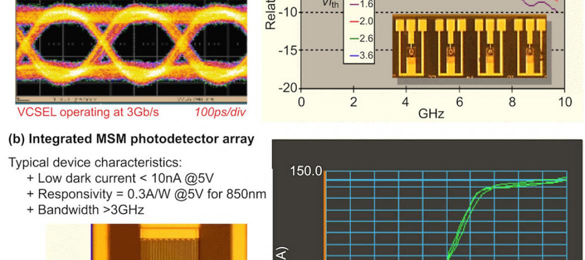
The POINT program was designed to leverage the electronic packaging and fabrication processes used at that time to significantly reduce the cost of optoelectronic packaging and to increase the chance of technology transition. These development efforts were focused on VCSEL-array devices and related packaging technology, passive alignment for the reduction of recurrence costs in optoelectronics packaging, polymer materials (i.e., Polyguide) for multimode board and backplane interconnect applications, and demonstration of a parallel optical link for backplane applications. The resulting prototype included an integrated 12-channel VCSEL array and a 12-channel metal-semiconductor-metal receiver (which had been developed under the DARPA-funded Optoelectronics Processing Components program).
