
Nanocavity Paves Way for Thinner Solar Panels, Optoelectronic Devices
Researchers have been looking for ways to improve energy absorption and transfer to improve photovoltaics and optoelectronics. We told you recently how scientists invented new energy-carrying particles to this end, and now researchers at the University of Buffalo (UB) are experimenting with nanotechnology to improve the design of ultrathin solar panels, video cameras, and other optoelectronic devices.
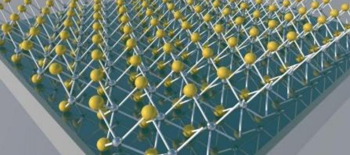
A team led by Qiaoqiang Gan, assistant professor of electrical engineering at UB’s School of Engineering and Applied Sciences, has developed an optical nanocavity made, from top to bottom, of molybdenum disulfide (MoS), aluminum oxide, and aluminum. MoS is a two-dimensional semiconductor commonly used in lubricants and steel alloys that has a bandgap structure similar to semiconductors used in LEDs, lasers, and solar cells.
A nanocavity, meanwhile, is an arrangement of mirrors that allows beams of light to circulate in closed paths. These cavities are used to help build things like lasers and optical fibers used for communications.
The team’s work with the nanocavity aims to solve an issue currently in demand to manufacture smaller, thinner, and more powerful optoelectronic devices. These devices also have smaller semiconductors, which do not absorb light as well as conventional bulk semiconductors. Makers of these products must sacrifice optical absorption capacity for a thinner form factor, said Haomin Song, an electrical engineering student who worked on the project with Gan.
“Industry has kept pace with the demand for smaller, thinner, and more powerful optoelectronic devices, in part, by shrinking the size of the semiconductors used in these devices,” Song explained. “A problem for energy-harvesting optoelectronic devices, however, is that these ultrathin semiconductors do not absorb light as well as conventional bulk semiconductors. Therefore, there is an intrinsic trade-off between the ultrathin semiconductors’ optical absorption capacity and their thickness.”
The nano cavity -- which engineers coated with a single layer of MoS molecules -- could potentially solve this issue and improve optical absorption even in thinner semiconductors, Gan said. This is because it can increase the amount of light that ultrathin semiconducting materials absorb.
