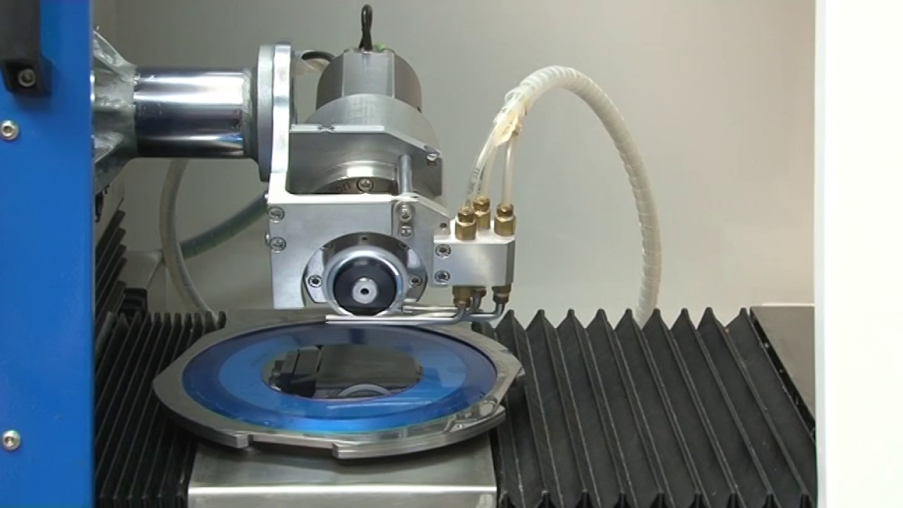
Wafer Sawing
In the context of manufacturing integrated circuits, wafer dicing is the process by which die are separated from a wafer of semiconductor following the processing of the wafer. The dicing process can involve scribing and breaking, mechanical sawing (normally with a machine called a dicing saw) or laser cutting. All methods are typically automated to ensure precision and accuracy. Following the dicing process the individual silicon chips are encapsulated into chip carriers which are then suitable for use in building electronic devices such as computers, etc.
During dicing, wafers are typically mounted on dicing tape which has a sticky backing that holds the wafer on a thin sheet metal frame. Dicing tape has different properties depending on the dicing application. UV curable tapes are used for smaller sizes and non-UV dicing tape for larger die sizes. Once a wafer has been diced, the pieces left on the dicing tape are referred to as die, dice or dies. Each will be packaged in a suitable package or placed directly on a printed circuit board substrate as a "bare die". The areas that have been cut away, called die streets, are typically about 75 micrometres (0.003 inch) wide. Once a wafer has been diced, the die will stay on the dicing tape until they are extracted by die-handling equipment, such as a die bonder or die sorter, further in the electronics assembly process.
The size of the die left on the tape may range from 35 mm (very large) to 0.1 mm square (very small). The die created may be any shape generated by straight lines, but they are typically rectangular or square-shaped. In some cases they can be other shapes as well depending on the singulation method used. A full-cut laser dicer has the ability to cut and separate in a variety of shapes.
Materials diced include:
- Glass
- Alumina
- Silicon
- Gallium arsenide (GaAs)
- Silicon on sapphire (SoS)
- Ceramics
- Delicate compound semiconductors

